caddesignsd.com All Rights Reserved | Website development by BIIS Solutions, LLC
Serving the electronics market, since 1991

- Preliminary quote can be given with schematic & board size
- Firm fixed quotes require
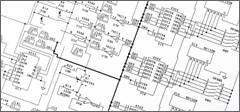
- Schematic
- Bill of Materials
- Board Size
- Special requirements:
- Number of layers
- Any special routing requirements
- Impedance and termination
- Differential pairs
- Length control and matching
- Placement restrictions
- Heat sinking
- Placement guidelines:
-
- Suggested placement if available
- Height restrictions
- Keep outs
- Parts grouping and associations
- Desired Lead Time (1 to 20 working days, depending on complexity)
- Estimated Start Date
PCB Design Quote Requirements
For quoting purposes it is not necessary to have precise, final data.
| Contact: | sales@caddesignsd.com |
| Phone: | 858-668-3505 |
| Fax: | 858-668-3504 |
| Address: |
4858 Mercury St. Ste.103
San Diego, CA 92111 |
| Phone: |
858-668-3505
|
| Fax: |
858-668-3504
|
| Email: |